




iWave Global iG-RainboW-G77M Versal AI Edge Gen2 SOM

iWave Global iG-RainboW-G77M Versal AI Edge Gen2 SOM has a form factor of 70mm x 80mm and provides the functional requirements for an embedded application. Three high-speed, receptacle, center strip contact connectors provide the carrier board interface to carry all the I/O signals to and from the iWave Global iG-RainboW-G77M Versal AI Edge Gen2 SOM.
Features
- SoC
- Versal AI Edge Gen2 SoC with SSVA2112 package
- Compatible with 2VE3858, 2VE3804, 2VE3558, 2VE3504 devices
- Processing system
- Arm® Cortex-A78AE application processor (up to 1.875GHz)
- Arm Cortex-R52 real-time processor (up to 875MHz)
- Arm Mali™ - G78AE with 4-core Graphics Processing Unit (GPU)
- Supports high speed interfaces like PCI Express Gen5 x4, USB 3.2, DisplayPort 1.4, 10G Ethernet
- Programmable system
- System logic cells up to 1,188K logic cells
- LUTs up to 543K and DSP Engines up to 2,064
- Supports AI Engine-ML v2 up to 144 tiles
- Supports 100G multirate Ethernet MAC and PLPCIE5 Gen5 for high-speed connectivity
- GTYP high-speed transceivers up to 32Gbps
- Memory interfaces
- 32-bit 4GB LPDDR5x for PS (expandable)
- Three 32-bit 4GB LPDDR5x for PL (expandable)
- 32GB eMMC Flash (expandable)
- 256MB OSPI Flash
- 4Kbit EEPROM
- 64GB UFS Flash (optional)
- PMIC - Renesas/Dialog’s DA9062 PMIC
- Other On-SOM features
- 10/100/1000 Ethernet PHY transceiver
- FAN header
- Power and status LEDs
- Power supply with 5V input through board-to-board connector
- Board-to-board interfaces
- From the PS block
- PS GTYP transceivers x4 up to 32Gbps (PCIe Gen5/10GbE/Aurora)
- GEM0 through on-SOM Gigabit Ethernet PHY
- RGMII x1(GEM1)
- One USB3.2
- One DP
- One USB2.0
- One SD (4-bit)
- One UART (Debug)
- One data UART
- Two I2C
- One SPI
- Two CAN FD
- One JTAG
- From the PL block
- PL GTYP transceiver x20 up to 32Gbps
- FPGA - X5IO Bank 710 with up to 16 LVDS/32 SE IOs and up to one pair of global clock input pins
- FPGA - X5IO Bank 711 with up to 15 LVDS/30 SE IOs
- FPGA - X5IO Bank 712 with up to 16 LVDS/32 SE IOs and up to one pair of global clock input pins
- FPGA - X5IO Bank 713 with up to 14 LVDS/28 SE IOs
- FPGA - X5IO Bank 706 with up to 16 LVDS/32 SE IOs and up to one pair of global clock input pins
- FPGA - X5IO Bank 707 with up to 9 LVDS/18 SE IOs
- FPGA - HDIO Bank 400/402 with up to 44 SE Ios and up to four pairs of global clock input pins
- -40°C to +85°C component’s temperature support
- RoHS and REACH compliance
- 70mm x 80mm (REN+ form factor) form factor
Applications
- Cloud to networking
- Wireless and wired communications
- Edge computing
- Endpoints
- Datacenter
- Test and measurement
Block Diagram

Development Tool
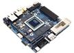
iWave Global iG-G77D® Versal™ AI Edge Gen2 Development Kit
Includes the necessary on-board connectors to validate the features of the Versal AI Edge Gen2 SOM.
Veröffentlichungsdatum: 2026-06-01
| Aktualisiert: 2026-06-02